Nanotechnology/STM
| Navigate |
|---|
| << Prev: Atomic Force Microscopy (AFM) |
| >< Main: Nanotechnology |
| >> Next: Scanning Near-field Optical Microscopy (SNOM) |
Scanning Tunneling Microscopy
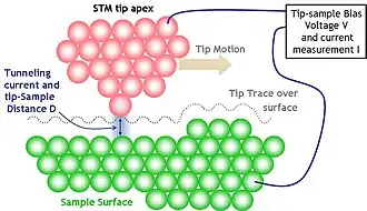
Scanning tunneling microscopy (STM) is based on the quantum tunneling effect, in which electrons can jump a short distance, even through a vacuum, between two conductive surfaces that are close enough to each other and above a certain voltage difference. In STM, a metallic probe sharpened to a single-atom point is brought to within a few nanometers from the surface that will be analyzed. This surface has to be conductive, so that a voltage differential between it and the probe can cause electrons to jump in between them, completing a circuit. There are two different modes for imaging: Constant height and constant current. In constant height, the probe is kept at a certain height, and changes in the current flow are measured as the probe scans horizontally. Constant current, on the other hand, moves the probe vertically while it is scanning so as to keep the current constant, and the vertical displacement is measured. Constant current is used mor often, as the surface does not have to be as flat as with constant height. The recorded data can then be used to make a map of the material's electron density, which correlates with its electrical properties and topography (heightmap).
Tips for STM
- KOH etched tungsten tips
- PtIr tips
References
See also notes on editing this book about how to add references Nanotechnology/About#How_to_contribute.