8

I have a question about how the BIOS is loaded and executed. I know that the CPU starts executing the BIOS at 0xFFFF0, but how is the BIOS there?

Is the BIOS hard wired to that address on the CPU, to where you can't overwrite it,

Or is it copied to that memory address, as if its just regular memory that you can read / write to.

If so, how does it get copied to that address if there's no existing program?

Context: I'm writing an emulator for a custom CPU and I want to know how the BIOS is stored and loaded in memory.

Giacomo1968
  • 58,727
Vinny
  • 91

10 Answers10

23

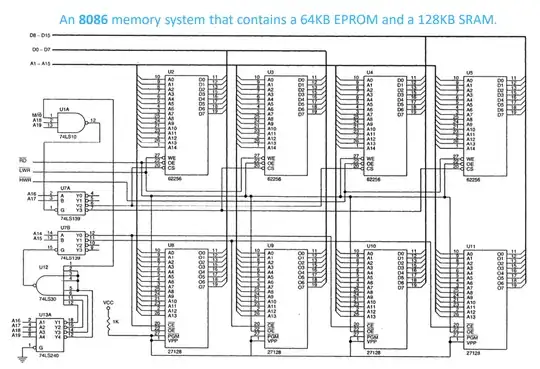
In the 8088/8086 systems this was typically done by physically mapping/connecting the A16-A19 lines to enable (via the 74138 chip enable/select lines) the right 74138-style decoder that was wired to the ROM chips enable lines. Other 74138s on the board had their chip enable/select lines wired differently, so the latter were enabled when address for the RAM were on the (address) bus. In that era, you also had multiple physical ROM chips (smaller than 64Kb), so that's why a decoder was used: lines A13-A15 were typically decoded by the same 74138 to select the ROM chip from the set.

Below is a diagram (source) of a somewhat complete memory system like that (the 139 is two 138s in the same package.) I suspect this is more an academic than real system: it uses 4x16Kb ROM chips (27128) in the lower half of the diagram, while the upper half of the diagram is the SRAM (62256 chips). The first real IBM PC used DRAM for RAM, so that's why this is more academic than real.

enter image description here


Or is it copied to that memory address, as if its just regular memory that you can read / write to.

That used to be called "shadow RAM" and didn't appear until the '386 era, I think. (N.B. There were some late 286 chipsets that had it too, e.g. VLSI 82C202 although some earlies ones e.g. 82C101 apparently didn't have it.) How that was done (in one [Headland] implementation):

When the system boots, a routine in the system BIOS makes a copy of the ROM modules to RAM by copying the BIOS back to itself. The [...] Memory Controller arranges the READ and WRITE operations in such a way that the ROM contents are duplicated in shadow RAM. [...]

The rest of the description is somewhat confusing [to me], but essentially it seems that the memory controller[s] of that era redirected ROM address writes to RAM, in that initial boot/copy mode. And then the BIOS switched the controller to "shadow mode", from which reads to those addresses were also served from RAM (after the copy was complete). Apparently in the latter/"shadow" mode, writes to ROM addressed were disabled/ignored [at the memory controller level], so the RAM-copy of the BIOS could not be changed in the aftermath. This was probably rather dependent on the memory controller though.

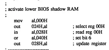
The bit that controlled the startup vs the later/"shadow" mode was somewhere in the I/O space, e.g. on that particular controller, after doing the self-copy, the BIOS routine had to do:

enter image description here

The 82C202 used a similar "self-copy" technique, but the write protection was independent in that one (and the I/O ports used to access the controller registers differed, of course.)

For clarity, there was nothing really specific to the '386 [or '286] processor in how the shadow mode worked. It was all at the [external] memory controller level. It's just that the feature didn't exist in the early IBM PCs, as far as I know.

10

The specifics of course would depend on the system design, but for example the IBM PC (which had the cheaper, but functionally similar 8088) had a 8kb ROM chip. This was hardwired to the upper memory addresses, as you suggested. So at reset the CPU would read straight from the ROM. Writing to the ROM memory space would obviously have no effect on the ROM content.

TrayMan
  • 203
7

Without complicating the answer, the BIOS or the firmware of a device isn't stored physically in the processor. There is a dedicated chip on a PCB to store it. The firmware is designed to check and initiate all the required tests and processes by "talking" to all the primary components on the PCB.

The firmware is initiated from the chip and brought to memory (RAM) for active use. The associated addresses on any other component on the device are merely addresses utilised by BIOS to run/initiate any processes it is required to do during start-up.


As you have edited and specified further information, I think the following existing posts may help you better understand, so I wont have to write it all out:

Giacomo1968
  • 58,727
Repaird
  • 449
7

To answer your question about the emulation, load the desired BIOS the the address where it needs to be (0x100000 minus size of your BIOS) before you start your emulated CPU at 0xFFFF0.

Background:

The 8086 (and compatible) start execution at address 0xFFFF0. It follows that there must be already a meaningful instruction (usually a jump to the start of the BIOS). The BIOS is not part of the CPU, because the BIOS is specific to the system. If there was a BIOS in the CPU, the CPU would be usable only in that system.

So providing the instructions for the BIOS is outside of the scope of the CPU, the system must provide these instructions to the CPU, before any initialization by the CPU can be done.

A common solution for that time was to provide the BIOS in a ROM chip. The 8086 has an address space of 1MB or 0x100000, so 0xFFFF0 is just below the top. When the CPU wants to read memory, it will place the desired address on the address bus, and the system must decide how to react this address based on the upper bits of the address. To select the ROM chip, you just need a decoder that detects that the top address bits are all set to 1, so a simple AND gate with a few inputs will do. How many bits are needed depends on the size of the BIOS. A BIOS with 8kB or 0x2000 will start at 0x100000-0x2000=0xFE000, so the top 7 address lines are needed to decode the 0xFE.

Access to ROM is quite slow, so later systems decided to copy the contents to RAM and then run the BIOS from RAM. but that didn't apply the to early systems. The original IBM PC came with 16kB RAM, extendable up to 64kB. It didn't make sense to waste 8kB RAM just to execute the BIOS faster. It also didn't make sense to waste the circuits necessary to implement this. As your emulator runs from RAM anyway, it doesn't make sense to implement something like that, unless you do it for the benefit of some existing software that expects it.

RalfFriedl
  • 1,734
4

BIOS was hardware mapped into the top 8KB of memory, and the processor read it from there, with all the associated extra wait states required by ROM accesses.

Original 8086 PCs didn't have enough spare RAM to copy the ROM into (Original only had 16KB RAM total), and even if they did, there was no hardware to remap RAM into the address space occupied by the ROM either.

I vaguely remember the BIOS was around 8KB (one of the IBM PCs I had, came with a listing(!) of the BIOS in the back of the ring bound manual).

Neil
  • 151
4

The iMC is exposed as a set of registers in the PCI(e) configuration space and/or MSR registers. Upon a reset the values of the registers (e.g. the SAD registers) controlling the standard hole (from physical address 0xa0000 to 0xfffff, included) default to not reclaiming any memory transaction.

When a core performs a load to, say 0xffff0, the iMC won't reclaim it. The load then reaches the System Agent that acts as the default destination (à là subtractive decoding like in a PCI bridge). If an internal PCI(e) reclaims such load, it is dispatched to it (e.g. the legacy VGA framebuffer). In this case, no sane PCI(e) would, so the System Agent sends the memory load down the DMI link.

Downstream the load reaches the PCH which, upon a reset, reads the (possibly virtual) strapon pins to know where the firmware flash ROM is located (typically through the SPI bus, or the LPC bus) and then reads the flash descriptor to find out the flash region and to default map the BIOS region just at the end of the 4GiB limit (where the PCI hole is located). Furthermore, by default, the PCH aliases the region just under 4GiB to 0xe0000-0xfffff.

So the load to 0xffff0 is aliased to 0xfffffff0, reclaimed by the ROM, and decoded to the appropriate offset.

As you can easily see, this is all by default.

As you go back in time the architecture changes but the principle remains the same. In the original 8086, there was probably just a simple shared bus and, as everybody with minimal knowledge of digital electronics knows, it's pretty easy to map devices at fixed addresses on a single shared bus (that's how the legacy IO port numbers arose).

It's worth noting that your understanding of an x86 booting is very far from the actual, modern thing. Not only modern x86s (not supporting x86S) boot with a CS base of 0xffff0000, but since Haswell, the first thing a CPU does upon an INIT is to fetch (through ucode) the FIT and execute the ACMs (which will eventually go back to the legacy boot).

Furthermore, it is usually the PCH that wakes up first and asserts the right pin/virtual wire to boot the CPU. The PCH firmware responsible for this is the BUP (Bring UP) and it's located in the same flash ROM of the CPU firmware (just in a different region). Since the flash ROM is attached directly to the PCH, it's easy to imagine how it's accessed.

Even before the PCH is powered, the BMC (Server), the SuperIO chip (desktop), or the embedded controller (laptop) is powered and these usually are ucontrollers (i.e. they have their internal ROM). So actually, that's plenty of possible software that runs before the first x86 instruction is fetched.

Finally, it was customary for the firmware to configure the iMC/NB to reclaim writes to the range 0xe0000-0xfffff and then read and copy this whole range to itself. Finally, the writes were routed back to the PCH (which, by default, won't route them through the SPI/LCP) and the reads were reclaimed instead. This had the effect of copying the firmware in memory, a thing known as shadowing.
Giacomo1968
  • 58,727
3

It can be read directly (some circuitry decoding the addresses can determine what memory to select to read from, depending on the actual address range) or it can be copied from ROM to RAM (called shadowing). There's no need for any program to do that, a dedicated (and rather simple) hardware circuit can simply loop through the address range and make the copying on startup, before letting the processor to start.

You might want to watch one or more of the series on YouTube of enthusiasts (eg. Ben Eater, James Sharman, Jack Oatley) creating 8-bit era microprocessors with discrete components. It's both entertaining and would also be very helpful in your case to really understand how these circuits actually work.

Addendum: because quite a few other answers and comments seem to view ROM shadowing as some complicated procedure that requires specific suppport from the processor and was unconceivable with 8086-era technology, this is a very simple hardware presentation, thanks to James Sharman (as mentioned above): https://www.youtube.com/watch?v=yR9cw7QehCg

Although I do hope the video will never go away from YouTube, to be consistent with the SE policy of self contained answers, a quick description: a counter iterates over the actual address range involved, addressing both ROM and RAM in sync. The ROM is wired to assert its data, the RAM to read it from the bus. As the counter reaches the end, its carry output triggers the additional circuitry to disable the ROM completely, to enable the RAM and to initiate the actual reset process of the processor.

Gábor
  • 286
2

I'm writing an emulator for a custom CPU and I want to know how the BIOS is stored and loaded in memory.

Emulating a CPU alone will not do you what you need, since the CPU does not determine what devices respond to its read and write requests.¹ You also need to emulate the RAM and ROM devices and the address decoding logic that decides what device (RAM, ROM, another device, or nothing at all) to enable for a read or write to a specific address.

Generally, a CPU sets up a request to read or write a particular address in its address space, which for an 8086 is addresses ranging from $00000 ("$" here meaning hexadecimal) to $FFFFF.² To do this it drives the address bus lines with the address sin question, drives some control lines to indicate e.g., whether it's doing a read or a write, and will be listening to the data bus for a read or driving it with data for a write.

All these signals are read by the address decoding logic which makes a decision, based on the particular signals, of which device (e.g., a RAM chip or a ROM chip) to select or enable. A simple system might enable a (large) RAM chip when A19 is low (i.e., all addresses from $00000-$7FFFF), enable a ROM when A19 is high and a read is requested, and enable nothing when A19 is high and a write is requested. (Doing that last bit is important; if it selected a ROM when the CPU was doing a write, both the CPU and the ROM would be driving the data bus which could potentially even damage one or the other.)

Address decoding logic can get pretty sophisticated: it can even include flip-flops (basically, switches that can be toggled by software) in the state it checks so that when the flip-flop is off you get one memory map, and when it's on you get another memory map. (This is, for example, how you can switch between ROM and RAM for a section of the address space.)

The Address Decoding page from the Wilson Mines 6502 primer is a nice tutorial about this, and even if you don't intend to do anything in actual hardware, it's worth reading it to better understand how address decoding works. (It doesn't matter that this is focused on a 6502 processor; the principles are the same for almost any processor.)


¹ Some CPUs do have on-board memory or other devices, sometimes a large enough set of these that it alone can function as an entire computer system; these are generally known as "microcontrollers" or "MCUs." But even here, it generally makes sense to treat these as logically separate systems and there will be internal address decoding for selection of particular internal functional units such as RAM, ROM and I/O devices.

² Actually, it can access almost 64K of addreses higher than $FFFFF, and additionaly has an I/O address space, but I ignore these here to keep the explanation simple. The same general principles apply regardless of these sorts of details.

cjs
  • 1,140
2

Think cost. In the era of the 8086 (think 1979-80), DRAM was still fairly expensive compared to ROM.

I'm not talking about EPROMs or even single-shot PROMs. I mean the lowest cost method, used by game cartridge manufacturers: sending out to a chip fab and having them make pre-loaded 8kb ROMs in quantity 10,000. This cost $5-10 each.

Whereas 16kb of DRAM was north of $100, I can't compare apples to apples here because 8kb DRAM wasn't really a thing.

0

The 0xFF..F0 address is specifically the address on the flash. However, the 0xFF...F0 is also an address in the CPU address range. It probably points to the SPI flash BIOS, but ultimately the exact details may differ from chip to chip.